The Electron Microscopy Unit is equipped with a transmission (TEM) and scanning (SEM) electron microscopes that can be used in a wide range of applications for analysis of biological, medical, environmental and material samples. These analyses include; Applications: The Electron Microscopes are scientific equipment used for research, teaching, training, industry and consultancy in biological, environmental and material science applications. These instruments are capable of simplifying atomic level structural analyses in biological and materials sciences as well as the semiconductor and pharmaceutical industries. 1. Life Sciences: 2. Materials Science Applications: 3. Nanotechnology Applications: Multidisciplinary field, which covers a vast and diverse array of devices derived from engineering, biology, physics and chemistry. These devices include nanovectors for the targeted delivery of anticancer drugs and imaging contrast agents. Nanowires and nanocantilever arrays are among the leading approaches under development for the early detection of precancerous and malignant lesions from biological fluids. These and other nanodevices can provide essential breakthroughs in the fight against cancer. A. Nanomaterial Applications: B. Life Science Applications: C. Semiconductor & IT Applications: D. Environmental Applications: 4. Semiconductor Applications: 5. Quality Control: 6. Scientific / Academic Research:
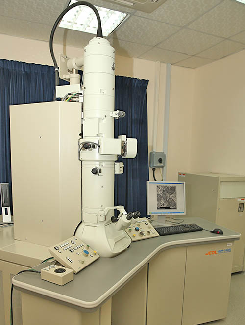
Equipment: Transmission Electron Microscope (TEM) The JEOL JEM-1400 TEM is an ultra-high magnification instrument offering state-of-the-art high contrast imaging up to x1,200,000 magnification with a high resolution of up to 0.2 nm for observing the internal structure (ultrastructure) of a specimen in micrometer (µm) and nanometer (nm) ranges. The system has the capability of exporting data to a dedicated tomography system for 3D structural elucidation. The specimen chamber has the capacity to load five samples at a time, 1mm3 biological samples are sliced into ultrathin sections from 60-90nm thickness using an ultramicrotome and then loaded onto Formvar carbon coated grids. The TEM uses an electron beam instead of light to study objects at high resolution. The electron beam is transmitted and focused through the sample section to create a 2D image in grey scale. The process of sample preparation is dependent on the sample type. Biological samples are first fixed to ensure there is no degradation using an automated tissue processor from RMC (EMP -5160), embedded in Araldite epoxy resin, and then sectioned using a RMS Power Tome Ultracutmicrotome XL to produce ultra-thin sections from 60-90nm if required. Inorganic geological samples do not require fixing however they still need to be prepared and then mounted on the Formvar carbon coated grids. JEOL JEM-1400 TEM with 3D Tomography System
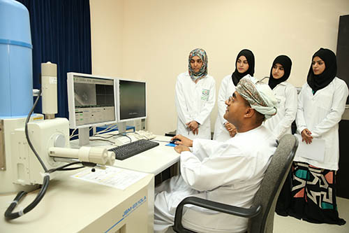
JEOL JSM-6510LA SEM with SED, BSD, and EDS detectors The JEOL JSM-6510LA SEM is capable of high magnification for observing the surface structure (topography) of a specimen in micrometer (µm) and nanometer (nm) ranges. The magnification is variable from x10 to x300,000 with a resolution of up to 3 nm. Unlike conventional light microscopes the SEM uses a beam of electrons to scan the sample; the reflected electrons are then detected using different types of detectors to create a 3D image in grey scale. The Preparation of sample depends on the sample type. The microscope operates at two modes; a high vacuum mode for which a treated sample must be used; and low vacuum mode where untreated sample can be used. Biological samples are fixed with Kamovsky's fixative to ensure there is no degradation, dehydrated in ethanol followed by Critical Point Drying using an autosamdri-815. The specimens are then mounted on stubs using carbon adhesive tape; finally they are Sputter coated with platinum particles using a JEOL JFC-1600 coater. Inorganic geological samples do not require fixing and dehydration however they still require coating with platinum to aid conductivity. The sample is then loaded into the sample stage and screened by using different detectors according to the requirements. Secondary electron detector (SED) produce topography imaging, Backscattered electron detector (BSD) produce sample compositional imaging. The X-Ray detector (EDS) is used for both qualitative and semi quantitative elemental analysis of the specimen, an image can also be generated showing the distribution of the elements within the sample topography.


